 |
 |
 | |||||||||||

How to do well in Assembly?
Date:2016-08-01
In PCB Assembly, there is a set of processthat is constantly being followed. One process cannot be skipped; one cannot beswitched to be performed over the other. For an SMT component populated PCB, itis always going to be the following processes (arranged in order):
Solder paste printing
Automatic placement
Reflow
But even if the processes are followed,certain problems arise when a populated PCB is inspected. In here, we are goingto tackle some of the PCB Assembly problems that are commonly encountered anddiscuss how to solve and prevent from happening again:
Solder bridging
Solder bridging is a phenomenon where atleast two neighbouring component pins have short circuited by way of anunnecessary solder. This phenomenon may be due to the following: excess soldervolume, inaccurate placement of the machine, or the plain mismatch of the PCBfootprint. To solve this problem, the engineers or assemblers should do thefollowing: reduce the solder volume by changing the printing machine settingsor go far as changing stencil mask opening.

2. Coplanarity
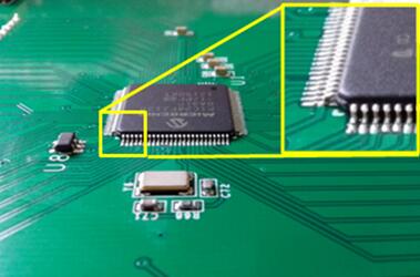
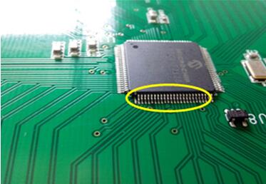
Coplanarity is a PCB Assembly problem thatcan be solved easily. This is mainly caused by a physically damaged component.But the cause of the damage will be difficult to find. It may be due to thedamage coming from the component supplier or a damage induced by the automaticplacement machine during the pick and place process. Either way, the focus ofthe investigation should only be concentrated on the component itself.

3. De-wetting
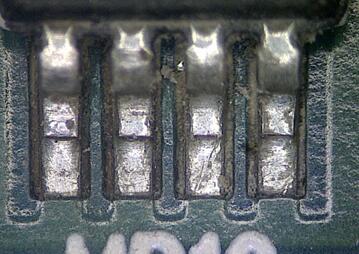
De-wetting is a solder anomaly wherein thecomponent pins don’t have enough solder creeping (wetting) around it. Itis also a common PCB Assembly problem. This may be caused by thefollowing: insufficient solder volume or mismatch of PCB footprint against thecomponent. To solve this problem, the engineer and/or the assembler must do thefollowing: change the solder volume deposit by changing the solder pasteprinting machine setting or change the stencil mask opening or change the PCBfootprint itself so it will match with component pins.

| Special |
 |
| About us |
| Prodcuts List |
| Our Capability |
| Factory Tour |
| Information |
| Contact us |
| News |
 |
| How to do well in Assembly? |
| 2016-08-01 |
 |
| Notice when you design the Multilayer PCBs |
| 2016-05-26 |
 |
| Our Location | ||||||
 | ||||||